Most read this week
-
 How do identical twins form? New insights reveal mechanism
-
 Peptides light up in the brain for early diagnosis of Alzheimer’s
-
 Could AI be the reason we haven’t encountered alien civilizations?
-
 Mushrooms could be the next big thing in energy storage
-
 Fluorine helps make PET plastic waste easier to recycle
Features

Stronger evidence links sedentary behavior and frailty in old age
Data gathered from hundreds of thousands of individuals finds strong link between sedentary behavior and becoming frail, simple changes can help.

Fluorine helps make PET plastic waste easier to recycle
Pre-activation of plastics with fluorine-containing molecules disrupts their stability, making them easier to break down and upcycle.

Could AI be the reason we haven’t encountered alien civilizations?
A sensational paper argues that AI could be responsible for the scarcity of advanced technological civilizations in the Universe.
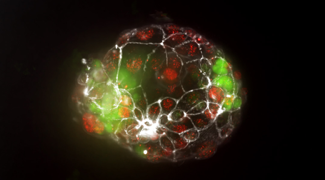
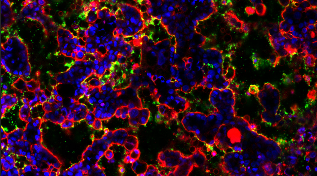
How do identical twins form? New insights reveal mechanism
A new organ-on-a-chip model allows researchers to study the splitting of the embryo during pregnancy for the first time.
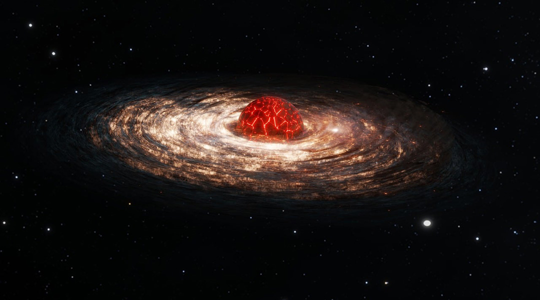
Hidden dark matter stars and where to find them
While dark matter’s enigmatic nature persists, Proca stars made of dark photons could help shed light on this cosmic mystery.
Stronger evidence links sedentary behavior and frailty in old age
Data gathered from hundreds of thousands of individuals finds strong link between sedentary behavior and becoming frail, simple changes can help.
Fluorine helps make PET plastic waste easier to recycle
Pre-activation of plastics with fluorine-containing molecules disrupts their stability, making them easier to break down and upcycle.
Could AI be the reason we haven’t encountered alien civilizations?
A sensational paper argues that AI could be responsible for the scarcity of advanced technological civilizations in the Universe.
Most read this week
-
How do identical twins form? New insights reveal mechanism
-
Peptides light up in the brain for early diagnosis of Alzheimer’s
-
Could AI be the reason we haven’t encountered alien civilizations?
-
Mushrooms could be the next big thing in energy storage
-
Fluorine helps make PET plastic waste easier to recycle
ASN Weekly
Sign up for our weekly newsletter and receive the latest science news directly to your inbox.
Research news

Electronic socks prevent foot-related complications in diabetic patients
An electronic sock detects an “unhealthy” walking style linked with diabetes and poor circulation to prevent foot ulcers and amputation.
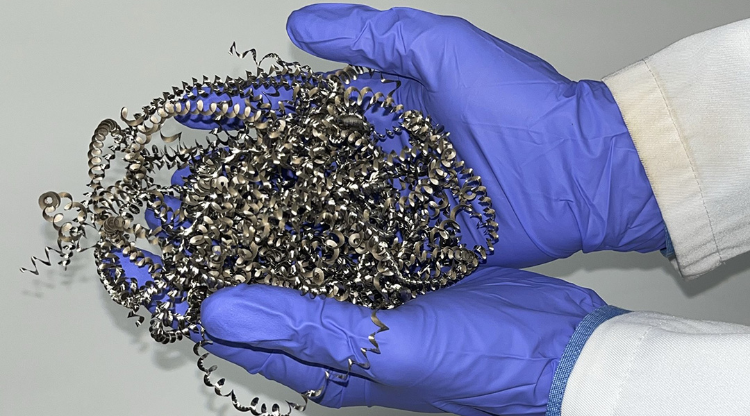
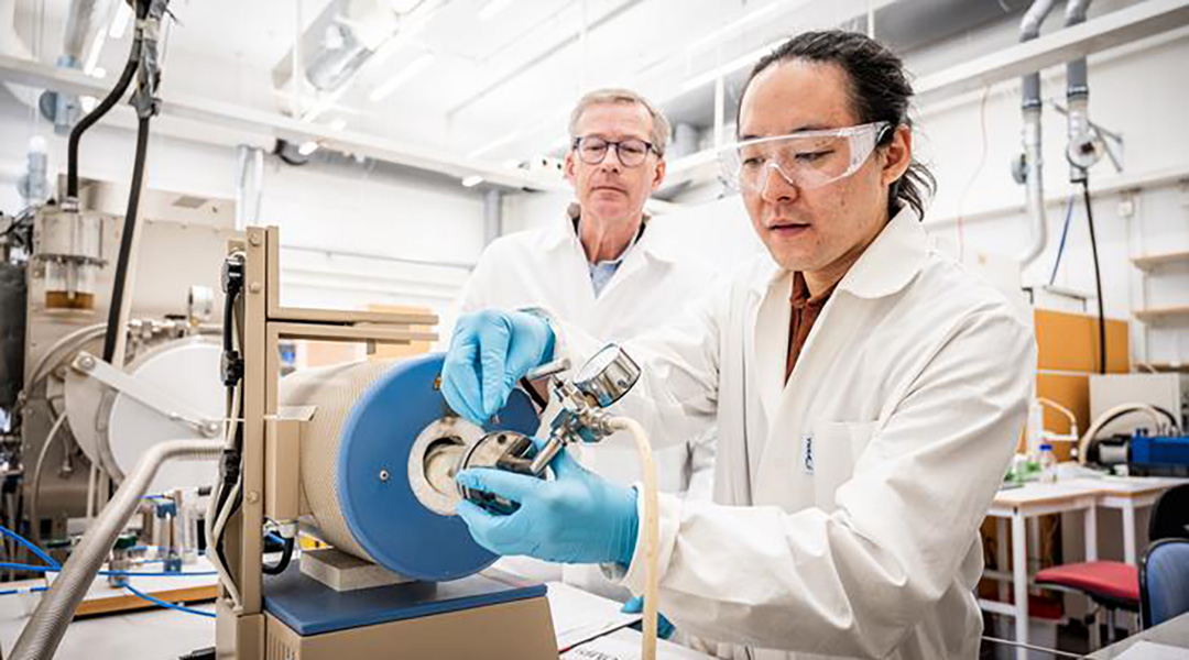
Turning industrial waste into clean hydrogen fuel
New technique uses waste metal shavings to catalyze hydrogen production, turning nothing but trash and water into clean, renewable fuel.
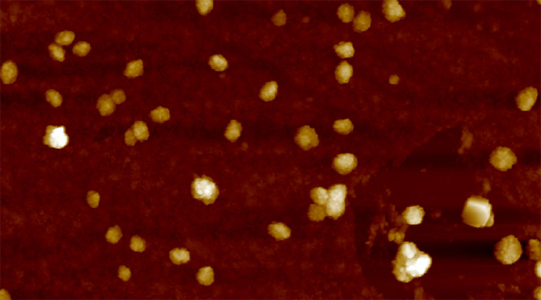
Goldene, graphene’s golden cousin produced for the first time
Scientists have managed to create sheets of gold only a single atom thick using a hundred-year-old Japanese smithing method.
Glass-like knee grafts help address donor shortage
A cryopreservation technique puts graft tissue into a glass-like state, preserving cells and viability during long-term storage.
Fluorine helps make PET plastic waste easier to recycle
Pre-activation of plastics with fluorine-containing molecules disrupts their stability, making them easier to break down and upcycle.

Laser light induces magnetism at room temperature
Scientists create magnetism in a non-magnet at room temperature for the first time, with implications in quantum tech and computer science.
Could AI be the reason we haven’t encountered alien civilizations?
A sensational paper argues that AI could be responsible for the scarcity of advanced technological civilizations in the Universe.
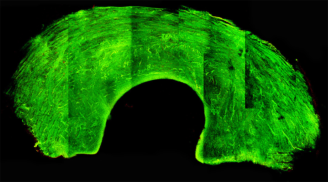
Peptides light up in the brain for early diagnosis of Alzheimer’s
Peptide-laden vesicles light up in the presence of amyloid beta, providing an early diagnostic test (and possible treatment) for Alzheimer’s.
Mushrooms could be the next big thing in energy storage
Scientists are using carbon filaments from mushrooms in supercapacitors, paving the way for a sustainable energy future.
How do identical twins form? New insights reveal mechanism
A new organ-on-a-chip model allows researchers to study the splitting of the embryo during pregnancy for the first time.

The decline of large river animals and the ecosystems now in peril
The decline of freshwater megafauna, including river dolphins, hippos, and crocodiles, is triggering significant consequences for ecosystems.
Hidden dark matter stars and where to find them
While dark matter’s enigmatic nature persists, Proca stars made of dark photons could help shed light on this cosmic mystery.

Indigenous fire management in Australia traced back 11,000 years
Abandoning traditional practices led to intense dry season fires, drastically altering biodiversity and increasing greenhouse gas emissions.
Research news
Electronic socks prevent foot-related complications in diabetic patients
An electronic sock detects an “unhealthy” walking style linked with diabetes and poor circulation to prevent foot ulcers and amputation.
Turning industrial waste into clean hydrogen fuel
New technique uses waste metal shavings to catalyze hydrogen production, turning nothing but trash and water into clean, renewable fuel.
Goldene, graphene’s golden cousin produced for the first time
Scientists have managed to create sheets of gold only a single atom thick using a hundred-year-old Japanese smithing method.
Glass-like knee grafts help address donor shortage
A cryopreservation technique puts graft tissue into a glass-like state, preserving cells and viability during long-term storage.
Fluorine helps make PET plastic waste easier to recycle
Pre-activation of plastics with fluorine-containing molecules disrupts their stability, making them easier to break down and upcycle.
Laser light induces magnetism at room temperature
Scientists create magnetism in a non-magnet at room temperature for the first time, with implications in quantum tech and computer science.
Could AI be the reason we haven’t encountered alien civilizations?
A sensational paper argues that AI could be responsible for the scarcity of advanced technological civilizations in the Universe.
Peptides light up in the brain for early diagnosis of Alzheimer’s
Peptide-laden vesicles light up in the presence of amyloid beta, providing an early diagnostic test (and possible treatment) for Alzheimer’s.
Mushrooms could be the next big thing in energy storage
Scientists are using carbon filaments from mushrooms in supercapacitors, paving the way for a sustainable energy future.
How do identical twins form? New insights reveal mechanism
A new organ-on-a-chip model allows researchers to study the splitting of the embryo during pregnancy for the first time.
The decline of large river animals and the ecosystems now in peril
The decline of freshwater megafauna, including river dolphins, hippos, and crocodiles, is triggering significant consequences for ecosystems.
Hidden dark matter stars and where to find them
While dark matter’s enigmatic nature persists, Proca stars made of dark photons could help shed light on this cosmic mystery.
Indigenous fire management in Australia traced back 11,000 years
Abandoning traditional practices led to intense dry season fires, drastically altering biodiversity and increasing greenhouse gas emissions.
How a gut-on-a-chip is getting to the bottom of our gut’s microbiome
This artificial gut will allow scientists to gain deeper insights into the biome that exists there and how dysregulat...

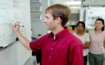
Athina Anastasaki: New ways to recycle old polymers
Polymer chemist Athina Anastasaki talks about establishing her career, inroads into polymer recycling, and resilience...

How research into existential risk will help safeguard humanity
Florian Jehn combines pragmatism with optimism when considering potential threats to human civilization.
...
Michael Dickey, our guide through the surprising world of liquid metals
The chemical and biomolecular engineer delves into the versatile applications, surprising properties, and future poss...
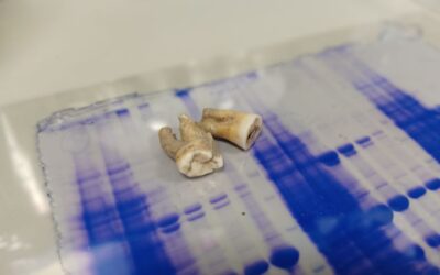
Centuries-old antibodies recovered from ancient teeth
Research teams from the UK have isolated antibodies preserved for 800 years in ancient teeth and found they are still...

It’s alive! How living materials are reshaping sustainable engineering
Discover how living materials are revolutionizing sustainable engineering, offering self-healing and responsive solut...
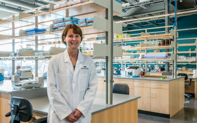
Unlocking the mysteries of the sea: A conversation with biochemist Andrea Bodnar
Andrea Bodnar, a biochemist by training, is leading researchers who strive to unlock the mysteries of marine life, pr...
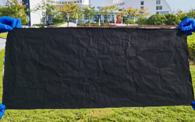
SPRABE: A stretchable, breathable, and self-adhesive electronic skin
Researchers create a multi-layered electronic skin that mimics human skin with applications ranging from robotics to ...

Can Dincer: “As a scientist, I love to be free”
Microsystems engineer Can Dincer builds disposable devices to enable personalized medicine.
...
Through the lens of rainforest conservationist and photographer Chien Lee
Not just pretty pictures: Borneo-based wildlife photographer and conservationist Chien Lee has a deeper message.
...
How a gut-on-a-chip is getting to the bottom of our gut’s microbiome
This artificial gut will allow scientists to gain deeper insights into the biome that exists there and how dysregulation can lead to disease.

Athina Anastasaki: New ways to recycle old polymers
Polymer chemist Athina Anastasaki talks about establishing her career, inroads into polymer recycling, and resilience in academia.
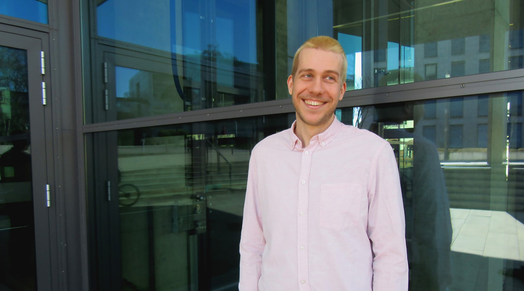
How research into existential risk will help safeguard humanity
Florian Jehn combines pragmatism with optimism when considering potential threats to human civilization.
Explainers
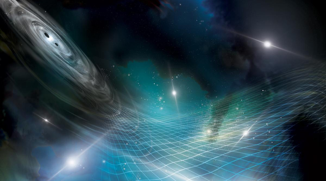
Understanding gravitational waves: Ripples in spacetime explained
The universe is ringing with gravity, but humanity is only just beginning to hear the nuance of this cosmic symphony.
What are neuromorphic computers?
To make computers faster and more efficient, scientists are using the brain as a model in this blossoming area of computer science.
What is quantum gravity?
Quantum gravity seeks to describe gravity according to the principles of quantum mechanics, but can it be done?
What is a black hole?
Regions of spacetime where gravity is so strong that nothing, not even light, can escape!
What are mRNA vaccines?
With a long history of development, mRNA vaccines are finally making their debut and changing the face of the COVID-19 pandemic.